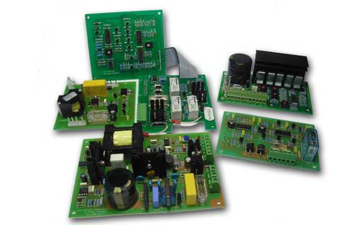
 The term reverse engineering is often misunderstood and associated with copying a circuit, this is not the case. The process of reverse engineering is much more complex and is reliant on the skills of the engineer undertaking the task to understand how the original system was designed to work and to identify possible design errors. Hopefully the following will help to explain the process. Ideally, one or more board that has failed in service should be supplied, together with details of its age and the environment that it is used in.
Stage 1 Schematic diagram
Produce a schematic circuit diagram from the sample PCB. From the schematic and sample PCB a full bill of materials can be produced.
Stage 2 Analyse the original design
Investigate the original design and check the original calculations to see if they were the possible cause of failure. Discuss with the customer any common failure modes they have experienced.
Stage 3 Redesign the circuit
Redesign any parts of the circuit that are likely to lead to failure, using modern techniques and components. Review the input and output interfaces to see if they can be protected from damage by other external circuit failures.
Stage 4 Analyse materials
Review the materials used and check if they are current and recommended for new designs. After many years there are usually alternative semiconductors, which are more reliable.
Stage 5 Design PCB
Utilising an industry standard PCB design software program, design a new PCB and apply the latest safety standards that are applicable to the product.
Stage 6 Sample manufacture and approval
Manufacture and test a sample product for customer approval. Following customer tests and formal approval, production assemblies may be produced.